


На сегодняшний день на рынке представлено много разновидностей металлоискателей разной ценовой категории, что значительно усложняет процесс выбора. Однако можно обратиться в специализированный магазин металлоискателей, либо совершить покупку через интернет магазин, где помогут подобрать подходящее устройство для ваших целей. Необходимо определиться с видом металлодетектора, так как именно он определяет область его применения.
Виды металлоискателей
Грунтовой
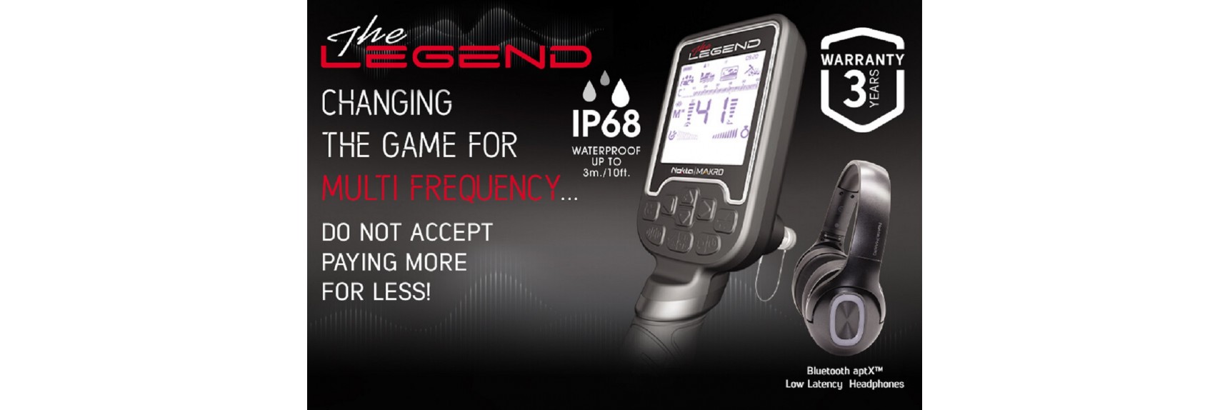
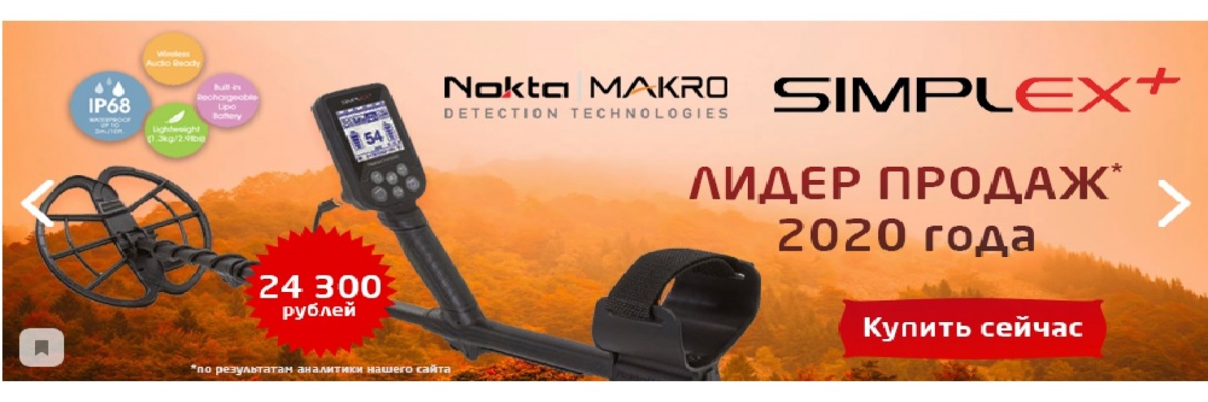
Самый распространенный поисковый магнит среди азартных сыщиков клада и цветного металла в грунте. Ассортимент металлоискателей данного вида очень широк и разнообразен. В основном, цена соответствует качеству. Чем дешевле модель, тем ниже точность и меньше глубина обнаружения металла. И, соответственно, определения материала металла тоже в них нет. Чем дороже металлоискатель, тем больше вероятности обнаружения даже мельчайших крупинок золота в земле на глубине до нескольких метров, с возможностью настройки на специальный вид металла.
Досмотровый
Используется, в основном, на таможенно-пограничных постах, для обнаружения под одеждой изделий из металла и оружия. Досмотровый металлоискатель допускается применять и в других сферах, где не важна высокая точность и большая глубина поиска. Досмотровый металлоискатель настроен только на поиск металла, вероятность установления размера и материи предмета не предусмотрены.
Данная модель прибора, в своей категории, является самым дешевым представителем.
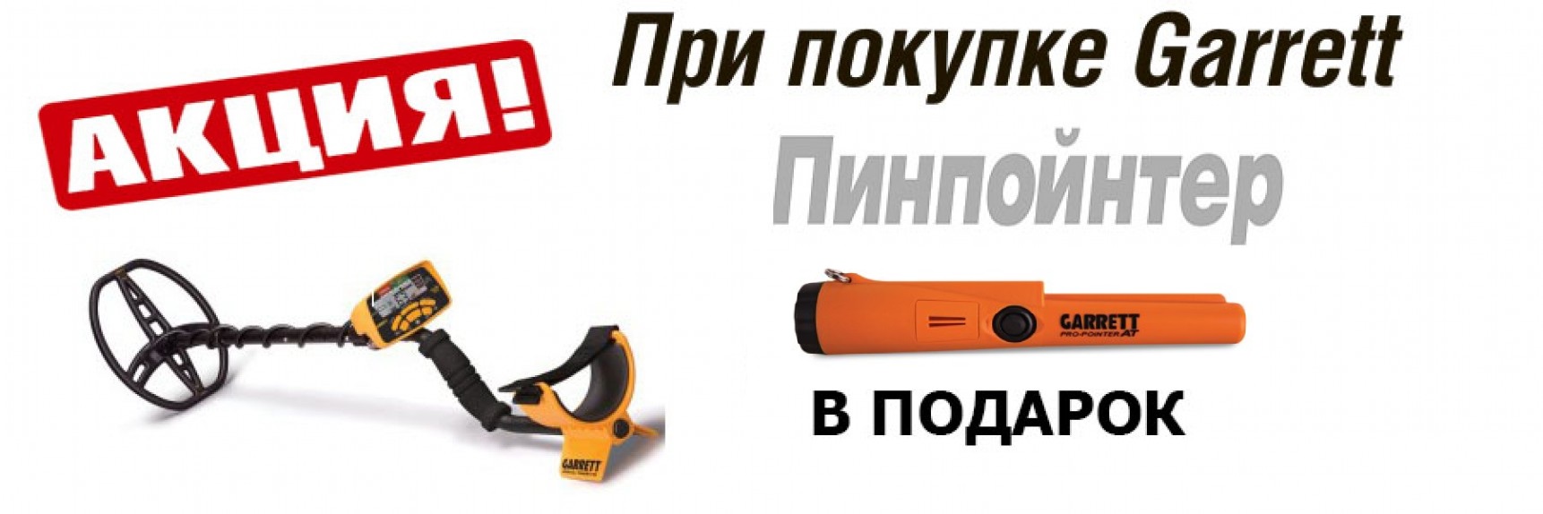
Пинпойнтеры
Аналогичны досмотровым металлоискателям по своим техническим характеристикам и незначительно отличаются в цене. Пинпойнтеры способны обнаружить металл в пределах небольшой площади и обладают возможностью обнаружения предмета на небольшой глубине. Обследовать большие помещения с данным металлодетектором затруднительно, но Пинпойнтер может локализовать место нахождения металла после работы грунтового металлоискателя.
Подводный металлоискатель
Металлоискатель по функциям полностью аналогичен грунтовому, но только герметичен и не боится длительного пребывания под водой. В подавляющем большинстве, подводный металлоискатель прекрасно справляется со своими функциями и на земле, вместо грунтового. Длину штанги и положение упора можно регулировать самостоятельно, в зависимости от вида работ – на земле или под водой.


